Diamond Processing and Nano-Patterning
Development of many diamond-based electronic and mechanical components relies on the ability to produce structures across a range of varied dimensions.
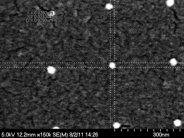
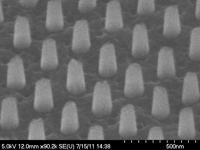
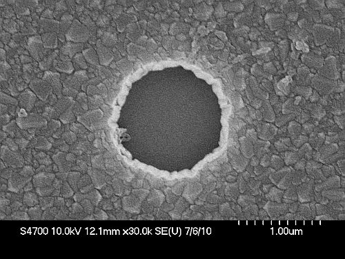
Utlising the range of facilities of the JWNC such as electron beam lithography, dry etching and metal/dielectric deposition, our work has established processing techniques for the formation of diamond devices and structures with dimensions ranging from hundreds of microns down to tens of nanometres. This includes processing of single-crystal substrates and polycrystalline diamond films.